
PCB Design
We know PCB layout and design.
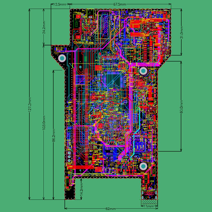
Successful PCB design for RF/Wireless applications presents many challenges and is an art as much as it is science. The PCB design must capture the RF hardware design, achieve isolation of high frequency signals from power supply and communication lines, provide for correct “RF” ground, isolate components that may be susceptible to crosstalk from other components, achieve dense component placement, provide for test point access—doing so within the space constraints dictated by the client’s enclosure while simultaneously creating a design that offers high yield during manufacturing. NextGen RF’s PCB design team are absolute experts in this field and deliver solutions helping our customers avoid the potential pitfalls for PCB design.
- Specialists for RF Design Layouts, RF Grounding and Shielding
- High Speed Digital, High Power, EMI/EMC Expertise
- 3D Modeling of PCBs and Components
- Altium, Mentor Graphics, OrCAD, Solidworks
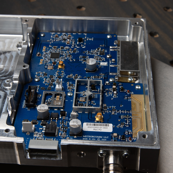
Train System High Power, High Linearity RF PA Board
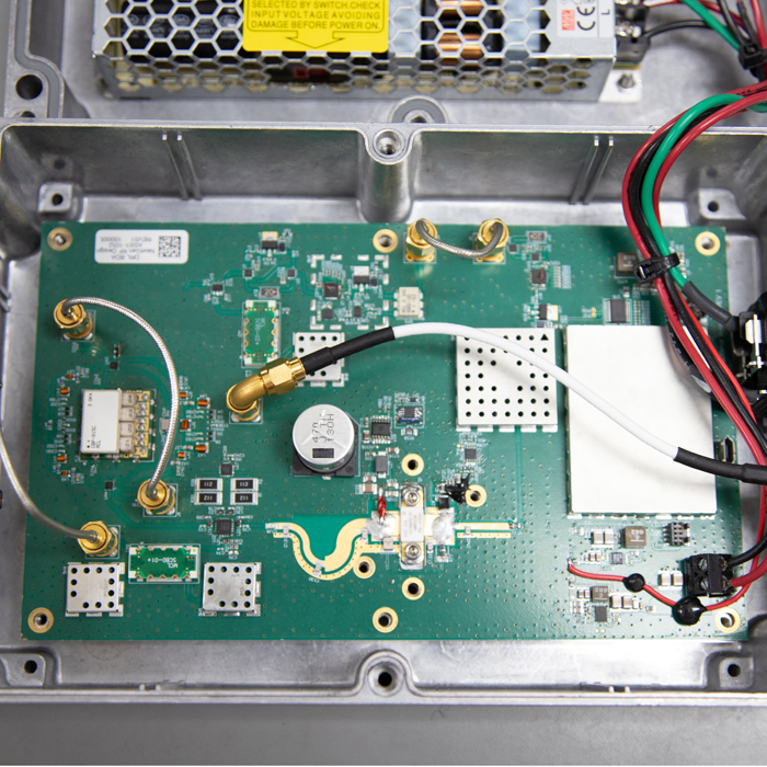
Bi-Directional Amplifier
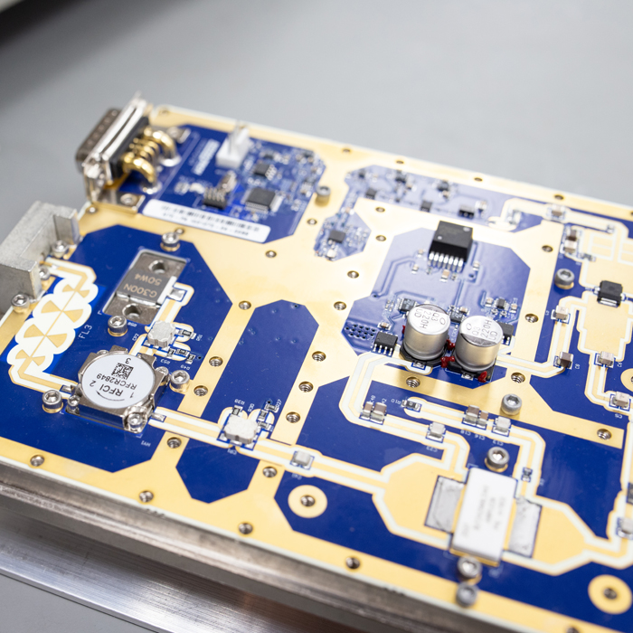
High Power Amplifier Board

Data Bus Matched Lengths Routing
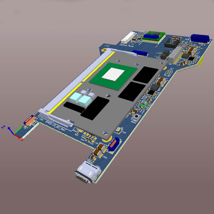
3D Model of PCB Circuit
High Density Interconnect
Why NextGen RF is the go-to partner for design, testing and fabrication.
Because we know design, NextGen RF has become the chosen partner or companies worldwide who require a high level of design expertise and responsiveness for their product development.
Making our clients happy, one project at a time.